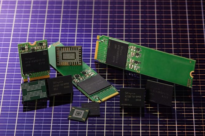
South Korean chip giant SK Hynix today launched, what it calls, 4D NAND memory. In reality today's announced 4D NAND product utilizes 96-layer TLC NAND with the logic circuits integrated in its own layer. The first chip that comes available has a storage capacity of 512 gigabits.
With the introduction of 3D NAND a new way to implement the logic to control the memory cells had to be designed. Intel and Micron discovered the most efficient way, which it calls CMOS Under Array (CUA). SK Hynix now developed its own method which it calls Periphery Under Cell (PUC). The benefit is that less chip area is required for the logic circuits, which means the same capacity will fit on smaller die-sizes, which ultimately results in lower costs per chip.
SK Hynix boasts that its technology reduces 30% of the chip size. Also performance is increased, with 30% faster writes and 25% faster reads.
The first end-user product that will feature the SK Hynix '4D NAND', will be a 1TB consumer SSD that should become available later this year. This drive will combine the 512 gigabits 96-layer TLC 3D-NAND chips from the South Korean chip giant with a controller and firmware that it also developed itself. An enterprise version of this SSD should become available in the second half of next year.
By that time, SK Hynix will also come with UFS 3.0 based NAND flash products. Later in 2019, the company will also roll out 96-Layer 1 Terabit TLC and QLC (Quad-Level Cell).


